For decades, tremendous progresses in semiconductor technologies have been making drastic changes in our life in various fields including computing devices, cell phones, digital photos, internets, and medical diagnosis technologies. Especially A.I. (artificial intelligence) technologies are going to grow and spread revolutionarily in the coming decade which are enabledd by further progresses in the nonvolatile memory embedded logic device semiconductor process technologies which heavily rely on nanoscale material science and chemical engineering.
Interconnects which are used to connect active devices electrically are basically just passive components in LSI chips. Nevertheless, the influence of the interconnect parasitic resistance (R) / capacitance (C) started to affect circuit performance adversely and seriously which has driven the semiconductor industry to the shift from aluminum interconnect to copper interconnect 21 years ago. The negative effect of interconnect RC on LSI chip performance (speed and power consumption) and reliability is getting worse as the down scaling proceeds to nanoscale. Pessimism that copper interconnect is no longer extendable to finer dimensions is accelerating exploration of alternative conductors such as cobalt interconnect and ruthenium interconnect.
Roles of science and technology in the field of chemical engineering have been already the central part of semiconductor manufacturing processes such as CVD (chemical vapor deposition), CMP (chemical mechanical polishing) for years. Accurate control for formation of desired material structures depends on diffusion control in the gaseous, liquid and solid phases, chemical reaction control, analysis of individual chemical step in various sequences of manufacturing processes (exemplified in Fig. 1). Synthesis of new chemical precursors and advanced materials for newly introduced processes is also mandatory for break-through of technologies.
In this talk, further contribution and emerging necessity of chemical engineering for break-through in interconnect technologies are overviewed.
Power semiconductor devices are key device to carbon-dioxide-reduction technologies. We focus on a SiC device with a wide bandgap, that operates with low loss and high efficiency at temperatures up to 300 °C. Conventional isolation and sealing technologies cannot cope with such high operating temperatures; therefore, new advanced materials are necessary. The KAMOME project was setup in 2011 to support material development and evaluation for high-current SiC power modules. This report presents the outline of the six-year KAMOME project. In the first two years of project KAMOME-I, the module designed as the platform was confirmed to be able to evaluate a full SiC module. We attempted to produce four types of platforms, PT-1 to PT-4. In the following two years, project KAMOME-II was conducted using a large-size SiC- Schottky barrier diode (SBD) of 9.54 mm2. Various encapsulating materials, electrical bonding materials, and thermal conductive sheets, which are under development, were evaluated using SiC power modules for the platform. Concurrently, a novel polymer alloy having both a high heat resistance and low thermal expansion coefficient was prepared by melt mixing of two compounds, bismaleimide diphenyl methane (BMI) and 3,3′-(methylen-1,4-diphenylen)-bis(3,4-dihydro-2H-1,3-benzoxazine) (P-d). The resin comprising BMI 1.0 and P-d 0.3 exhibited superior thermal properties and processability compared to other combinations. When the compound was cured at 200 °C for 4 h, the glass transition temperature of the resulting product was > 300 °C. An encapsulation material was prepared using this polymer alloy and compared with those of conventional epoxy materials. In the final two years, KAMOME-III, by designing a simple package especially for the packaging techniques and materials, we could achieve a high evaluation accuracy with short routines. A package applied high heat-resistant encapsulation resin provided from participant companies, passed 50,000 cycles in a power cycle test with Tjmax = 225 °C and ΔT = 160 °C from 65 °C for the cooling temperature. A most excellent thermal conductive sheet maintained a stable heat transfer property for the SiC module after heating at 175 °C, 200 °C, and 250 °C for 500 h, respectively. In this project, 64 companies collectively participated mainly in developing the materials.
There are numerous joints in electronic products. The properties of the joints are crucial to the products' reliability. Several interesting and unexpected phenomena are observed at the joints of electronic products, such as polarity effect caused by electromigration and liquation caused by interfacial reactions. The uneven growth of the Ag3Sn phase in the Sn/Ag couples, i.e. polarity effect, was reported 20 years ago for the first time, and was realized to be caused by electromigration effect. Electromigration effect remains as an important but not fully understood effect in the electronic products. Unexpected liquation could be disastrous to the reliability of electronic products. The liquation phenomena encountered at the Sn-Sb/Ag, Cu/Bi2Te3 and γ-InSn4/Ni are illustrated. The unexpected melting of the Sn-5at%Sb solder was resulted from the excess intake of Ag from the substrate during first-step soldering, and an Ag-Sn low-melting eutectic was formed during the second-step soldering. The Ag-(Sn-5at%Sb) isoplethal section is used for illustration. The extremely fast dissolution rate observed in the Cu/Bi2Te3 couples at 350 °C was caused by the formation of liquid phase. Cu reacted with mostly Te in the Bi2Te3 substrate to form the Cu2Te phase, the excess Bi became a separate phase and was molten at 350 °C. It is illustrated with a Bi-Cu-Te isothermal section. The peculiar microstructure observed along the γ-InSn4/Ni interface was a result of two competing processes. When a compound of less indium was formed due to interfacial reactions, the solder became indium-rich, its melting point was lowered and a liquid phase was formed. This phenomenon and could be understood with a In-Sn-Ni isothermal section.
Critical dimension of semiconductor device has been reduced to 10nm level recently and the demand for atomic level processing is increasing. In this work, atomic layer etching processes were developed for silicon oxide and silicon nitride and applied to surface cleaning applications. This work can potentially replace conventional wet cleaning processes that are facing limitations due to the reduced dimension in nanometer scale and transport limitation of cleaning solutions. In this work, we developed and characterized plasma atomic layer etching process for SiO2 (native oxide) removal in an inductively coupled plasma (ICP) reactor. The process consists of two steps of a surface modification step and a reactant removal step. In the first step, SiO2 surface is modified with fluorocarbon polymers generated with CHF3, C4F8 or C3F7OCH3. In the second step the fluorinated oxide is removed with ions or radicals generated from Ar, or O2 plasma. Ion energy is controlled typically less than 100V. Formation of fluorocarbon polymer layer on SiO2 surface was confirmed by SEM and XPS analysis. The removal rates were controlled under 10 â/cycle by controlling plasma powers and reaction gas flowrates. Self-limited characteristics was confirmed in the removal rate showed self-limited characteristics as the processing time increases. The effect of surface cleaning was confirmed from metal-oxide-semiconductor devices fabricated on the cleaned surface of nanoscale patterns.
Two-dimensional (2D) transition metal dichalcogenides (TMDCs), such as MoS2, have attracted considerable attention owing to the unique optical and electronic properties related to its 2D ultrathin atomic layer structure. MoS2 is becoming prevalent in post-silicon digital electronics and in highly efficient optoelectronics due to its extremely low thickness and its tunable band gap (Eg = 1-2 eV). For low-power, high-performance complementary logic applications, both p- and n- type MoS2 field-effect transistors (FETs) must be developed. n-type FETs with an electron accumulation channel can be obtained using unintentionally doped n-type MoS2. However, the fabrication of MoS2 FETs with complementary p-type characteristics is challenging due to the significant difficulty of injecting holes into its inversion channel. Plasma treatments with different species (including CF4, SF6, O2, and CHF3) have also been found to achieve the desired property modifications of MoS2.
In this work, we demonstrated a p-type multilayer MoS2 enabled by selective-area doping using CHF3 plasma treatment. Compared with single layer MoS2, multilayer MoS2 can carry a higher drive current due to its lower bandgap and multiple conduction channels. Back-gated MoS2 p-type FETs were presented with an on/off current ratio in the order of 103 and a field-effect mobility of 65.2 cm2 V-1s-1. The MoS2 FETs exhibited UV photodetection capability with a rapd response time of 37 ms and exhibited modulation of the generated photocurrent by back-gate voltage. This work suggests the potential application of the mild plasma doped p-type multilayer MoS2 in UV photodetectors for environmental and human health monitoring.
In the present paper, by experimentally examine the diffusion equation derived from magnetohrdrodynamic (MHD) theory, formation process of the vacancy layer was clarified.
Ionic vacancy is a polarized free space of the order of 0.1 nm surrounded by oppositely charged ionic cloud, which arises from the conservations of momentum and electric charge during electron transfer [1].
When elctrochemical reaction is carried out with vertical MHD electrode under a vertical magnetic field, the radial current distribution on the electrode yields a macroscopic solution flow like tornado rotation. Its centrifugal force produces a pressure toward the electrode center, inducing the center-oriented secondary flow. As a result, the rich layer of ionic vacancies that is formed on the center makes the electrode surface free without friction and gives rise to a specific flow without viscosity.
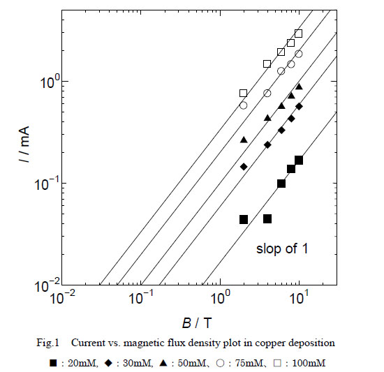
From theoretical calculation, depending on whether the electrode surface is rigid or free, two types of limiting diffusion current equations were obtained, Ii=LiBCs2 for i = ri or fr, where the subscripts ri and fr imply the rigid and free surface, respectively. B is the magnetic flux density, and Cs is the bulk concentration.
In Fig. 1, the plot of current vs. magnetic flux density in copper deposition is shown. Obtained data of Li = 4.1×10⁻⁸A mol-2 m6 T-1 was compared with the calculated data of rigid surface Lri , which was consistent with each other. However, in case of free surface, Lfr also provided the same value when the collision coefficient of ionic vacancy was 0.44, so that we cannot discriminate the difference. On the other hand, the increase of the current rising potential shift with cupric ionic concentration, which strongly suggested the formation of the vacancy layer.
References
[1] R. Aogaki, et al., Sci. Rep., 6, 28927 (2016).
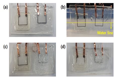
In this study, we present the disposable electronic circuit based on the pH-responsible encapsulation layer. Disposable electronic devices have been attracted because it can be discarded after we use it. This disposable property could provide advanced utilization for security, privacy issue, and implantable biochip. Meanwhile, it is an unavoidable problem that the electronic functions are deteriorated with the conventional disposable electronic device when they are exposed to water or severe circumstance. To tackle this issue, controlled disposable materials have been researched. However, it has still suffered from malfunction of the electronic device under external water. In this report, we newly developed pH-responsible encapsulation layer to overcome the aforementioned issue. The encapsulation layer could be stable and robust at acidic and neutral water environment, resulting in functioning as the expected electronic circuit without malfunction. Meanwhile, it is dissolved at base water solution and thereby, it can be totally disposed to small molecules. To prepare the pH-responsible encapsulation layer, we synthesized POC prepolymer through a condensation reaction. The POC prepolymer solution was coated to a glass substrate and then cured at elevated temperature. The cured POC film was stable at acidic and neutral water solution. However, it was totally resolved PBS buffered base water solution. We also fabricate electronic circuit on POC film substrate. It can be functioned when it is folded below 25 mm of bending radius. Finally, we studied a synthesis of a novel pH-responsible film of POC and investigated dissolving mechanism under PBS buffered water solution.
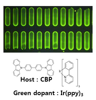
In this study, we demonstrate the effect of polymer guest of the inkjet printing of OLED device. Inkjet printing of OLED materials has been an attractive process because of on-demand pixel formation, resulting in less using OLED materials. However, it is challenging to obtain the highly uniform thin film quality similar to the one achieved by a conventional thermal evaporation process. Due to the coffee ring effect, an inkjet-printed ink droplet evaporates non-uniformly, leading to coffee rings. To control the coffee ring effect, we investigate the effect of UVO treatment of the substrate surface, the temperature of baking, and a solvent mixture of inks solution. To do this, we prepared home-made inkjet printer. This printer has 16 nozzles of inkjet head and exhibits dispensing 10 picoliters of an ink droplet from each nozzle. We also prepared pixel bank layer of 80 ppi pixel resolution. The OLED inks were filled in the pixel banks accurately by using our homemade inkjet printer. We varied the inkjet printing speed, ink droplet spacing, and waveform of piezo pump of inkjet nozzle in order to explore the thin film quality. It was observed that ink droplet itself was significantly affected by waveform of piezo pump. By varying waveform of piezo pump, the outgoing velocity, diameter, and satellite of ink droplet was changed. Moreover, the thin film quality of ink droplet depended on the spacing ink droplet. From this, we obtained thin film of OLED with uniformly controlled surface. Finally, we studied organic thin film layer, deposited by an inkjet printer, with the 3D surface analyzer and atomic force microscope.
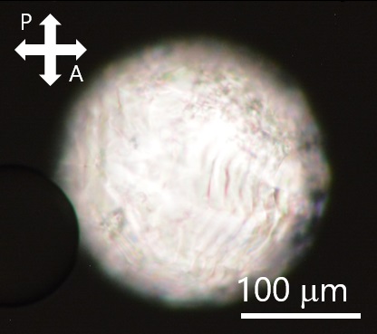
Since the ferroelectric state of a chiral smectic C (SmC*) phase stabilized in a thin flat glass cell was reported, SmC* materials have been attracting a great deal of attention due to possibilities for electro-optic devices such as displays with higher responsivity than present displays consisting of nematic materials. Although the ferroelectric states of the SmC* phases in the thin flat glass cells have been well investigated, the induction of ferroelectricity in spherical microcapsules has not been reported yet. A variety of liquid crystalline (LC) microcapsules can be precisely fabricated by using glass capillary microfluidic devices, which enables us to fine-tune the shell thickness. The difficulty of the fabrication of SmC* microcapsules is attributed to their high viscosity owing to the order of molecular layer in the SmC* phase. To apply the LC materials with high viscosity to the microfluidic devices at room temperature, we developed a new method. We named this method “ELIXIR method” in which the LC-to-isotropic (Iso) phase transition is induced by the addition of a certain volatile organic solvent “elixir.” Here, we present the fabrication of SmC*microcapsules using ELIXIR method and the molecular alignment there.
For the first time, we successfully fabricated SmC* microcapsules with about 15-μm shell thickness at room temperature by using acetone as the elixir (Figure). The addition of acetone induces the SmC*-to-Iso phase transition so that the viscosity of the SmC* material becomes suitable to the microfluidic fabrication. Moreover, we successfully align the molecules by dissolving acetone in the outer aqueous phase for annealing. The obtained SmC* microcapsules show broken fan-shaped textures with periodic stripes (Figure) that come from the helical structure in the SmC* phase. We will try to unwind the helical structure to induce a ferroelectric phase in the future.
In recent decades, metal nanomaterials for printing technologies has been widely investigated to develop compact, lightweight and cost effective electronic device such as solar cell, organic light emitting device, and thin film transistor. Among various metal nanomaterials, copper nanoparticle has attracted considerable attention due to its excellent electrical conductivity (~105 Scm-1) and thermal conductivity as well as relatively low cost compared with other metal nanomaterials. Despite these merits, it is limited for practical use owing to its easy oxidation in ambient condition. To prevent oxidation of copper, several groups have suggested such as coating with air stable materials (novel metal, organic surfactant, and carbon). However, this approach required expensive and complex process as well as it is necessary to remove protective layer when it applied to electrical circuits.
There have been many studies to prevent corrosion of steel by cathodic protection effect of electro-conducting polymer. In particular, Grgur groups reported polyaniline (PANI) are effective for anti-corrosion of steel when it was introduced to steel, because there was oxygen reduction reaction on the PANI instead of corrosion of steel.
Herein, we report novel approach to improve air-stability of copper by cathodic protection effect induced from copper/PANI composite. At first, PANI with emeraldin based (EB) form was prepared by self-stabilized dispersion polymerization. Subsequently, copper was deposited on PANI-EB powder by a wet reduction method to synthesis copper/PANI composite. The characterization such as morphology, microstructure, and conductivity of resulting composite was analyzed. In addition, the effect of PANI on air-stability of copper was also demonstrated.
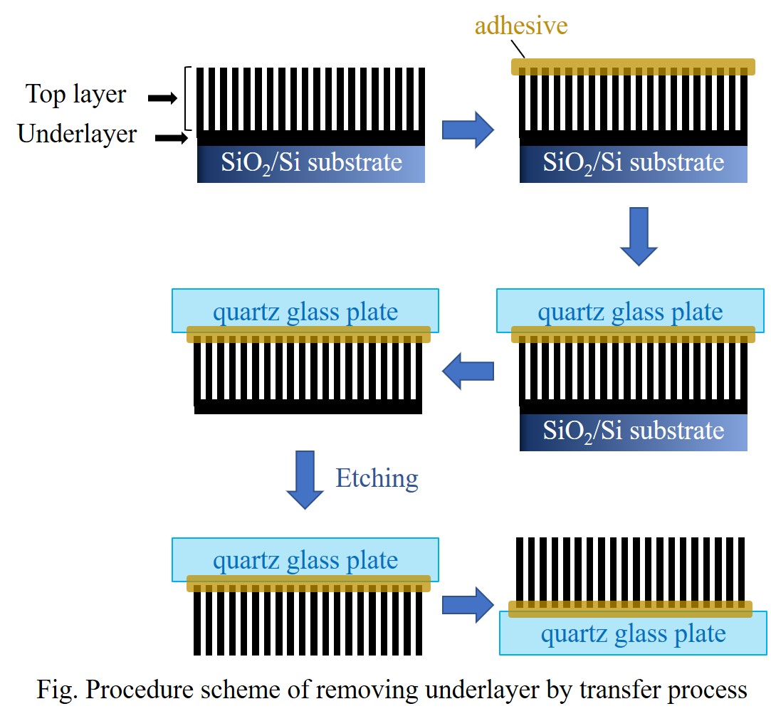
In this study, we synthesized parallel carbon nanowall and fabricated anisotropic conductive films by transfer process. The parallel CNW can have electrical resistance anisotropy, and its application to ACFs could be expected. However, in our previous study, the electrical resistance anisotropy of parallel CNWs is insufficient for application to ACFs. Therefore, we tried to improve the electrical resistance anisotropy by transferring CNW and removing the underlayer.
The synthesis of CNW was carried out using ECR plasma CVD. Carbon monoxide and hydrogen gas wwere introduced into the system and decompressed to 50 Pa, high density plasma was generated by 2.45 GHz microwave and the magnetic field of 875 G created by the coil. CNW was synthesized on a SiO2/Si substrate placed in the lower part of the waveguide.
The synthesized CNW was transferred to a quartz glass plate using an adhesive.
Etching of CNW underlayer after transfer was performed using ECR plasma. Using the same apparatus as CNW synthesis, Ar and H2 were introduced at a ratio of 2: 1, pressure 50 Pa, microwave 2.45 GHz, magnetic field density 875 G and ECR plasma was generatedand etching was performed.
In order to measure the properties of CNW as ACFs, the transmittance and the electrical resistance were measured at each etching time, and the electrical resistance was measured using the four-probe method.
Since the substrate is colorless and transparent, it is considered that the change in transmittance of CNW corresponds to the change in deposited carbon, and the electric resistance change with etching time is compared with the change in transmittance. It was shown that the amount of change in electrical resistance per etching amount was larger for transferred CNW than that of untransferred one, which suggested that the contribution to the electrical resistance of the underlayer was large.
Health monitoring has been an important issue in modern life. Among many media for health monitoring, sweat is a good one because it is rich in many chemicals from our bodies and offers a non-invasive way for sampling. In this study, we develop a printed and wearable device for sweat ion sensing with AC sources, and the data can be transmitted to smartphone by Bluetooth.
The wireless sensor contains a pair of interdigital electrodes, a signal IC processor, and a wireless transmitting circuit. The relationship between the AC impedance of the electrode and the ion concentrations in sweat is first characterized as a calibration curve. The electrode is then connected to a portable and wireless impedance measurement system to realize real-time monitoring. A skin-affinitive microfluidic system will be fabricated to effectively collect sweat on skin for the AC analysis, or salt concentration measurement. Effects of water evaporation, applied AC frequency, and applied voltages, on the accuracy or sensitivity will also be examined carefully to optimize the sensing system. In summary, this study demonstrates the possibility of applying AC measurements to detect total ion concentration in sweat, and the versatile sensing platform can be further extended to other wireless detection systems.
The present study reports the effect of copper (Cu) doping in CdS QDs to improve the photoelectrochemical performance of quantum dot sensitized solar cells (QDSSCs). Cu-doped CdS photoelectrode was prepared by successive ionic layer adsorption and reaction (SILAR) method on FTO substrate and used directly with CuS counter electrodes (CEs) and a polysulfide electrolyte. The changes observed in the diffraction patterns of Cu-doped CdS thin films suggest that Cu dopant can introduce increased disorder into CdS material structure. The surface morphology of Cu-doped CdS photoelectrode indicate that the fragments are uniformly distributed with high crystallinity. The photovoltaic current density – voltage (J-V) characteristics of Cu-doped CdS photoelectrode shows the specific improvements in open circuit voltage decay (Voc), short-circuit current density (Jsc), and fill factor (FF) under the illumination of one sun (AM 1.5 G, 100 mW cm-2), which is higher than the values of undoped CdS thin film based QDSSCs.
Light-emitting electrochemical cells are the future generation of flat-panel displays and solid state lighting sources. Compared to conventional solid state lighting device such as organic light-emitting diode (OLED), light-emitting electrochemical cell (LECs) possess simple device architecture and air stable electrodes makes LECs more impressive. Mainly LECs are two types, p-LECS and Ir-ITMCs. Currently much research has been focused on cationic iridium complexes due to the phosphorescent, color tuning and an ionic nature of Ir-ITMCs. However, the source and expensive nature of iridium demands new emitters in LECs. Recently non-ionic small molecule light-emitting electrochemical cell were reported by Tang et al. The molecule which is an ionic apart from Ir-ITMCs has great attentions. We designed and synthesized an ionic small molecule having strong luminescence and good charge transporting capabilities. A complete structural, photophysical, electrochemical and electroluminescent properties were investigated. Blue light- emissions were achieved by applying the target compound in a LEC device.
The ability to monitor cardiovascular system in real time is essential for patients with cardiovascular diseases. Electrocardiograph (ECG) usually becomes the first choice to provide an important information for monitoring. Flexible pressure sensors have attracted great interests in recent years due to their multiple applications including touch screens, electronic skins and biomedical diagnostic sensors. Many groups have contributed to increasing sensitivities of flexible pressure sensors over the past decades. However, the flexible pressure sensors are still limited to low sensitivity and spatial coverage on detecting targets. The aim of this paper is to present the flexible capacitive pressure sensors with high sensitivity that are able to measure the small magnitude of contraction. To detect such subtle movement, capacitive sensors therefore require a dielectric material which can be easily compressed resulting a quickly respond and release for pressure sensing. The sensitivity of capacitive pressure sensor can be improved by integration of micropatterns on the contacted surface. The dielectric micropatterns can be generated by using photolithographic technique to enhance the precision and consistency. Different potassium hydroxide (KOH) etching conditions were tested to obtain multiple size of pyramidal pits on silicon molds. In this study, we used the polydimethylsiloxane (PDMS) as a flexible dielectric material, therefore, the pyramidal micropatterns can be easily transferred from the silicon mold. These pyramidal micropatterns have the features with a base from 10.45 to 63.31 μm, periodic spacing from 6.87 to 50.16 μm, and with sharp or blunt tips. The dielectric film with micropatterns was coated with silver nanowires or ITO as the electrode and sandwiched between PDMS or PET substrates. The results demonstrate that the sensitivity of the capacitive pressure sensors increased with pyramidal micropatterns. We believe this flexible capacitive pressure sensor has potential to become a powerful tool for implantable medical applications.
Polyimides are already widely used in aerospace, automobile, electronics and other high-technology areas based on their excellent mix of properties. Expectations are that colorless polyimides will rapidly take hold and that their use will encompass what we now consider to be futuristic applications. The trick is to come up with the right combination of building blocks, creating a recipe where the formulations are not only developed, but are balanced and optimized. We herein report on a new class of polyimide (PI) nanohybrid substrates based on highly fluorinated asymmetric diamines as a building block of PI backbone structure. The resulting PI nanohybrids were highly soluble in polar aprotic solvents and displayed excellent optical properties, including high transparency (>91% at 400 nm), low refractive index (<1.5589), and very small birefringence (<0.0025 at 637 nm). The results provide useful information for designing molecular architectures for manufacturing high-performance flexible substrates in future display devices.
Here, highly stretchable and transparent UV cured poly (urethane-acrylate) elastomer has been synthesized by reacting urethane acrylate oligomer and reactive diluents monomers. The synthesized elastomers can be stretched up to 600% and have high transparency of over 90% transmittance. The morphology of poly (urethane-acrylate) elastomers was characterized and evaluated by FTIR and XRD as well as the thermal properties were examined and analyzed by TGA and DSC. The mechanical, optical and surface properties were analyzed by UTM, UV-Vis spectrophotometer. To verify the applicability of the poly (urethane-acrylate) elastomer, 3D printing, polymer ionic conductor and UV cured foam were studied. The elastomers are evaluated as the best materials for not only conventional applications but also for new applications.
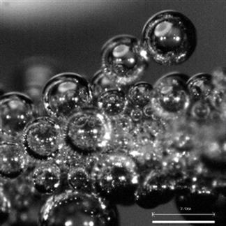
Alkaline water electrolysis (AWE) is anticipated as an important technology for conversion of electric energy generated from renewable energy obtained from wind power and solar power to hydrogen gas. To improve the hydrogen production efficiency of AWE, characterization and control of bubble generation behavior near electrodes is important. This study developed a system for measuring microbubble generation behavior on electrodes using a combination of microscopic technique and a high-speed video camera. The relation between the hydrogen or oxygen bubble size and the current density – electrode potential curve was investigated using electrodes of different diameters.
Three-electrode electrochemical cell experiments were conducted using nickel wires (0.3 or 0.1 mm diameter) as working electrodes, nickel rods (3 mm diameter) as counter electrodes, and a reversible hydrogen electrode (RHE). The electrolyzer was made of polyvinyl chloride, with four sapphire windows covered by PMMA. Electrolytes were 2 M KOH. Generation behavior of micrometer size bubbles of hydrogen and oxygen near the working electrode was recorded at 12,000 frames per second with full resolution using a high-speed video camera. Cyclic voltammetry was used at a 10 mV/s scanning rate using an electrochemical measurement system.
Results show that oxygen bubbles formed from anode electrodes are 40–300 μm. Hydrogen bubbles formed from the cathode electrode are 30–100 μm, and are smaller than oxygen bubbles, although the hydrogen generation volume is twice that of oxygen. Oxygen and hydrogen bubbles become larger with both the current density and electrode diameter. Oxygen bubbles on the anode electrode coalesce and become large especially under high current density conditions.
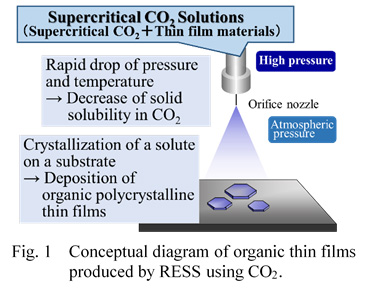
Organic thin film transistors (OTFTs) have been established as one of the most promising materials for future thin, lightweight, and flexible electronic devices. Device performance is strongly dependent on the molecular structure, morphology, and properties of the thin films of organic semiconductors from which they are formed. Because conventional methods for the deposition of organic thin films including vacuum deposition methods and solution methods have some drawbacks, new approaches are required to produce high-quality thin films with large grain sizes and smooth surfaces. We have proposed a novel and simple deposition technique of organic thin films by rapid expansion of supercritical solutions (RESS) using CO2, as shown in Fig. 1, and have successfully produced thin films of some organic semiconductor materials on SiO2/Si substrates. Furthermore, a fabricated top-contacted OTFT with a tetracene or TIPS-pentacene layer was activated. However, carrier transport characteristics of the current OTFTs using RESS are not good enough for practical application. One of the reasons for the low carrier transport characteristics is that the thin films produced by RESS are polycrystalline thin films. Improvement of carrier transport characteristics of the OTFTs, therefore, is one of the important approaches for practical application of RESS.
In this work, we focus on Ph-BTBT-10 as a TFT material because the TFT using polycrystalline thin films shows high mobility. We report deposition of Ph-BTBT-10 thin films on SiO2/Si substrates by RESS using CO2, and the crystal and electrical characterization. Scanning probe microscopy showed that the thin films consist of a high density of submicron-sized grains. X-ray diffraction showed that the thin films had regular arrangement structures in both the horizontal and the vertical directions of the substrate. A fabricated top-contacted OTFT with the Ph-BTBT-10 active layer showed p-type transistor characteristics with a field effect mobility of more than 0.1 cm2/V s.