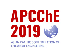
Poor stability and reproducibility of perovskite solar cells (PSCs) have prevented the devices from practical applications of industrial standard photovoltaic modules that can withstand sustained long-term operation under outdoor conditions. Furthermore, most of presented high efficiency PSCs utilize halogenated antisolvents such as toluene and chlorobenzene to assist perovskite crystal growth with large grain-size, excellent coverage and high uniformity, but they are highly toxic and detrimental to environment. To solve such issues, we developed simple methods for the production of functional nanocomposites such as Ag-rGO, perovskite-NiO, perovskite/Ag-rGO, NiO-carbon-graphite, etc and utilized them for the fabrication of ambient-air and antisolvent-free processed stable, hysteresis-free PSCs. In addition, to solve interfacial degradation whcih affects device performance Al2O3/NiO layers were utilized for interface engineering between elecrtron transport layer and active layer. By introducing the functional composites into PSCs with interface engineering, we obtained high efficiency of > 18 % and fill factor of > 78 % with excellent reproducibility. More importantly, the devices without encapsulation showed significant enhancement in long-term stability and the photovoltaic parameters sustained its stability over 330 days with retaining over 95 % of its original values under ambient condictions (see Fig. 1).
Silicon tandem solar cell is one specific type of multi-junction solar cell, which has the potential to exceed the efficiency limit of single-junction silicon solar cell and eliminates the lattice mismatch found in hetero-junction type. The porous silicon (PSi) is a potential candidate as a top cell due to its wider bandgap, which is originated from quantum size effect, for higher Voc and low reflectance leading to enhancement of light absorption.
However, the surface area and defects are highly increased compared to crystalline Si (c-Si). Therefore, suitable passivation is necessary to reduce surface recombination. The representative method to passivate silicon solar cell is atomic layer deposition (ALD). However, the cost of ALD is too high to be widely used. In this research, a low-cost electrochemical passivation technique was developed for achieving uniform passivated layer on PSi.
In this study, the PSi with porous thickness of 200-250 nm was fabricated through anodization process in HF solution. The photoluminescence (PL) was measured to observe the bandgap of P-type PSi. Then it was passivated by either electrochemical passivation in HCl or ALD (Al2O3) to compare the carrier lifetime and nanostructure. Finally, solar cell performances of electrochemical passivated samples were measured.
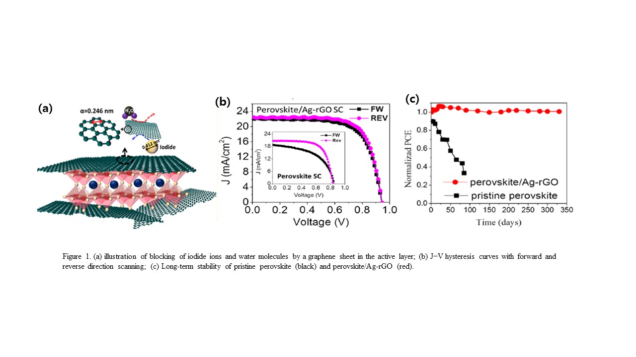
The result of solar cell performance shows the improvement of Jsc and efficiency of PSi solar cell compared to c-Si; the 30 seconds electrochemical passivated PSi yielded 29.8 mA/cm2 and 10.7%, and the c-Si yielded 23.4 mA/cm2 and 8.2%, while both Voc are not much different. However, the PL data shows that the bandgap is increased from 1.1 eV (c-Si) to 1.9 eV. Therefore, in order to improve Voc, the surface passivation and configuration of front electrode are key factors to reduce recombination and increase lifetime. Also, the relationship of porous structure and pn-junction depths is important.
To reduce the cost of Monocrystalline Si solar cell and the amount of Si by thinning the wafer with keeping high efficiency is promising approach. A major method to obtain monocrystalline thin film Si is the epitaxial growth by Chemical vapor deposition(CVD) and layer transfer process. Si is epitaxially deposited on a seed layer such as double layer porous Si(DLPS) with top seed layer and bottom sacrifice layer. The rate and the yield of epitaxy by CVD and the defect level caused by the roughness of the seed layer were critical issues. We developed the method to fabricate high quality film by smoothing the surface of DLPS within nanometer level with zone heating recrystallization(ZHR)[1] that selectively heat the surface by scanning of lamp heater. Also we developed rapid vapor deposition(RVD)[2] to get the high deposition rate over 10 μm/min by heating Si source over 2000 °C. By applying these methods, we obtained the monocrystalline Si in 3 min and the critical effect of lowering the roughness of DLPS in less than 0.3 nm is confirmed[3][4].
In this work, to fabricate high quality solar cell, we (1)investigated the key factors to change the roughness of DLPS and (2)evaluated the semiconductor properties of monocrystalline thin film Si. The surface smoothing of DLPS were inhibited by oxidation and by changing the atmosphere to H2/N2 promoted the decrease of the surface roughness. After modifying the method to fabricate over 35 μm thin film Si by RVD in one time, the thin film Si with passivation Al2O3 film on both sides by ALD showed the sufficient life time as monocrystalline Si film by the life time measurement.
[1]A.Lukianov et al.,Appl.Phys.Lett 108(213904)1-4(2016)
[2]Y.Yamasaki et al.,CrystEngComm 18-3404-3410(2016)
[3]C.Takazawa et al.,ECS.Transaction 75(31)-11-23(2016)
[4]K.Hasegawa et al.,CrystEngComm.in press20(2018)1774-1778
Recently, nanosheets (NSs) have been attracted attention owing to their various unique properties. The synthetic methods of NSs are divided into two categories: top-down exfoliation methods and bottom-up methods. However, both methods have some problems. As one of the former methods, NSs can be obtained from the exfoliation of layered materials; the thickness of the obtained NSs are a few nm, but this method can be applied only to layered materials. As one of the latter methods, NSs can be obtained from the chemical vapor deposition on a smooth substrate; this method can synthesize NSs of various chemical compounds, but the NSs are not so thin. It is required to develop a versatile method to synthesize thin NSs.
We focused on the two-dimensionally confined space in a bilayer of hyperswollen lyotropic lamellar (HL) phases of amphiphile solutions as a sandwich-like reaction fields (SRFs) for the synthesis of thin NSs; HL phases are classified as one of lyotropic liquid crystalline phases. The SRFs with several nm thickness are separated from each other by about several hundred nm. In fact, NSs were successfully synthesized in the thin hydrophobic SRFs inside the bilayers of aqueous amphiphilic solutions. The thickness and horizontal width of the NSs are a few nm and several hundred nm, respectively. The thickness of the obtained NSs is almost constant. We have developed such a synthesis method and named it "two-dimensional reactors in amphiphilic phases" (TRAP) method.
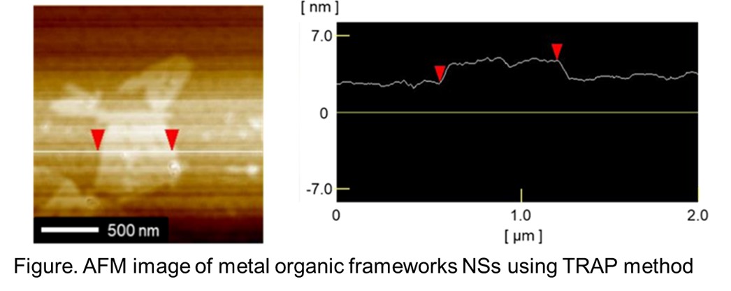
Here, we present the NSs synthesis using TRAP method. We confirmed that TRAP method can be apply to the hydrophobic materials made from both hydrophilic and hydrophobic ingredients such as metal organic frameworks (Figure). Furthermore, we found that it is possible to synthesize NSs in the thin hydrophilic part of the SRFs.
Surface modification plays an important role in determining interfacial adhesion between substrate and electroless-deposited (ELD) metal layer. In this presentation, we will share our experience regarding to control of surface modification on either organic or inorganic substrate and its relation to the adhesion strength of subsequent ELD metal layers. In particular, case studies of adhesive ELD on silicon wafer, glass sheet, Ajinomoto build-up film and photoimageable dielectric will be reviewed. It is concluded that with sufficient control of surface modification, the adhesion strength of ELD layer can be largely enhanced due to formation of either covalent bond or donor-acceptor-like interaction.
